


The circuit board is an elementstructure, which consists of a dielectric base and copper conductors, which are applied to the substrate in the form of metallized areas. It provides the connection of all electronic circuit elements.

The printed circuit board has a number of advantages in comparison with volumetric (hinged) mounting using cables and wires:
The circuit board also has drawbacks, but there are very few of them: limited maintainability and high complexity of adding design changes.
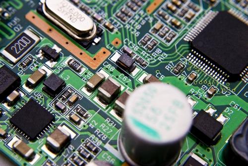
Elements of such boards include: dielectric base, metallized coating, which is a picture of printed conductors, contact pads; fixing and mounting holes.
The requirements for these products are GOST
To improve the corrosion performance andincrease the solderability of the surface of the board is covered with an electrolytic composition, which must be continuous, without peeling, tearing and tanning. Fixing and mounting holes must be placed in accordance with the drawing. It is allowed to have deviations determined by the accuracy class of the board. In order to improve the reliability of soldering on all internal surfaces of the mounting holes, a layer of copper is deposited, the thickness of which must be at least 25 microns. This process is called - the metallization of holes.

Что такое классы печатных плат?This term implies the classes of accuracy of board manufacture, they are stipulated in GOST 23751-86. Depending on the density of the picture, the printed circuit board has five accuracy classes, the choice of which is determined by the level of the technical equipment of the enterprise. The first and second classes do not require high-precision equipment and are considered cheap in production. The fourth and fifth classes require special materials, specialized equipment, ideal cleanliness in production facilities, air conditioning, maintaining the temperature regime. Domestic enterprises mass produce printed circuit boards of the third class of accuracy.


